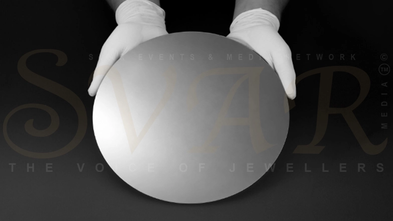
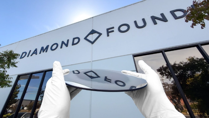
Diamond Foundry has created the world’s first 200mm single-crystal diamond, marking a significant breakthrough in advanced materials and semiconductor technology. Developed after 25 years of scientific research and engineering innovation, the D200mm single-crystal diamond could open new possibilities in AI computing, high-performance electronics, thermal management and wafer-scale semiconductor manufacturing.
Quick Summary
- Diamond Foundry has created the world’s first-ever 200mm single-crystal diamond.
- The D200mm crystal is one continuous diamond measuring 200mm in diameter.
- The achievement follows 25 years of scientific research and engineering efforts led by Stefan Gsell and Martin Fischer.
- Both scientists joined Diamond Foundry in 2022 through its acquisition of Augsburg Diamond Technology (Audiatec).
- Diamond’s exceptional thermal conductivity and mechanical, electrical and optical properties make it promising for advanced technology applications.
- The breakthrough could support future developments in AI computing, high-power electronics, semiconductor manufacturing and thermal management.
- Diamond Foundry’s achievement establishes a pathway towards wafer-scale diamond manufacturing and the potential development of D300mm substrates.
Diamond Foundry Creates the World’s First 200mm Single-Crystal Diamond, Marking a New Era for Semiconductor Technology
After 25 years of scientific research and engineering innovation, Diamond Foundry has achieved a major breakthrough with the creation of the world’s first 200mm single-crystal diamond, opening new possibilities for semiconductor manufacturing, AI computing and advanced technology applications.
Diamond Foundry has announced a significant milestone in materials science with the successful creation of the world’s first-ever D200mm single-crystal diamond. Measuring 200mm in diameter, the achievement represents a major advancement in the manufacturing of diamond as a technology material at semiconductor scale.
Unlike conventional diamond crystals, the newly developed D200mm is one continuous single crystal. The breakthrough demonstrates the potential to manufacture large-format diamond substrates for next-generation semiconductor and advanced technology applications.
Diamond is recognised for its exceptional combination of physical properties, including the highest thermal conductivity, outstanding mechanical strength, electrical insulation, optical performance and potential for extreme electronic capabilities. These characteristics have long positioned diamond as a promising material for future technologies. However, its limited crystal size has remained one of the biggest challenges to its wider industrial adoption.
With the development of the D200mm single-crystal diamond, Diamond Foundry has taken an important step towards overcoming this longstanding limitation.
Why Scaling Diamond Manufacturing Matters
The semiconductor industry’s development has been closely connected to its ability to manufacture advanced materials at increasingly larger wafer sizes. Silicon’s transition towards larger wafers transformed electronics manufacturing, enabling more sophisticated semiconductor devices to be produced with greater economic efficiency and consistency.
Diamond, however, has historically faced significant manufacturing limitations. While natural diamond formation remains dependent on geological processes, conventional laboratory-grown diamond production has generally been restricted to comparatively smaller crystal dimensions.
As the demand for advanced materials continues to grow across high-power electronics, artificial intelligence computing, optics and quantum technologies, the limited size of single-crystal diamond has remained a major obstacle.
Achieving diamond growth at the 200mm scale required significant advancements in plasma physics, reactor engineering and manufacturing process control. The milestone reflects years of scientific experimentation and engineering development aimed at making large-scale single-crystal diamond production possible.
25 Years of Scientific Research and Perseverance
The achievement is the result of a scientific journey spanning 25 years, led by Stefan Gsell and Martin Fischer, who have dedicated their research and engineering efforts to developing high-quality single-crystal diamond with scalable dimensions.
Both scientists joined Diamond Foundry in 2022 following the company’s acquisition of Augsburg Diamond Technology (Audiatec). Their expertise in diamond crystal growth was subsequently combined with Diamond Foundry’s reactor technology and manufacturing capabilities, strengthening the company’s efforts to advance large-scale diamond production.
Commenting on the breakthrough, Martin Roscheisen, CEO of Diamond Foundry Inc., highlighted the collective contribution of the company’s engineering and scientific teams.
“This is one of those milestones that once seemed almost impossible,” said Martin Roscheisen, CEO of Diamond Foundry Inc. “Hundreds of DF engineers, scientists, and technicians contributed to us getting here. It is the accumulated result of countless experiments, failures, inventions, rebuilt machines, and insights over more than a decade.”
Roscheisen also acknowledged the extraordinary perseverance demonstrated by Stefan Gsell and Martin Fischer throughout their 25-year pursuit of the scientific challenge.
“Stefan and Martin pursued this goal for 25 years,” Roscheisen said. “There are very few examples in technology of someone sticking to a really hard scientific challenge with that level of perseverance. They kept going when the prevailing view was that single-crystal diamond simply could not be made at this scale. Today, the perseverance shows as the first-ever D200mm single-crystal diamond. And best of all, it makes D300mm predictable as well.”
The breakthrough has been supported by developments across multiple areas of technology and manufacturing, including plasma generation, growth chemistry, reactor architecture, crystal engineering, thermal management, metrology, automation and manufacturing processes.
What the 200mm Diamond Breakthrough Means for AI and Computing
The development of D200mm forms part of Diamond Foundry’s broader vision to transform single-crystal diamond from a scarce material traditionally associated with gemstones into an industrial semiconductor substrate that can be manufactured at scale.
The achievement comes at a time when advanced computing systems are facing increasingly complex thermal management challenges. Modern artificial intelligence processors generate substantial amounts of heat as enormous computing power is concentrated within extremely small areas of silicon.
Managing this heat efficiently has become a critical consideration in semiconductor performance, reliability and future chip architecture.
Diamond’s exceptional thermal conductivity offers significant potential in addressing these challenges. Its ability to efficiently spread heat at the material level could create new opportunities for advanced chip designs, higher power densities, improved reliability and more effective cooling systems.
Beyond AI computing, the material’s combination of thermal, mechanical, electrical and optical characteristics could support innovation across several next-generation technology applications.
Building the Foundation for Wafer-Scale Diamond Manufacturing
Diamond Foundry is developing single-crystal diamond for semiconductor and advanced technology applications where its unique material properties could enable performance beyond the limitations of conventional materials.
The successful development of D200mm demonstrates a pathway towards overcoming the crystal-size limitations that have historically restricted diamond’s industrial applications.
The company’s achievement also points towards the possibility of progressing to D300mm diamond substrates, representing another important milestone in the development of wafer-scale diamond manufacturing.
Reflecting on the significance of the achievement, Roscheisen emphasised the importance of the people and long-term scientific commitment behind the breakthrough.
“Technology history is often written around the moment something finally works,” Roscheisen said. “But that moment rests on the people who were willing to spend years, sometimes decades, making it work. This diamond exists because hundreds of people contributed, and because a few people refused to give up on the idea for 25 years.”
A New Chapter in Advanced Materials and Semiconductor Technology
The creation of the world’s first 200mm single-crystal diamond represents more than a manufacturing achievement. It marks an important development in the evolution of diamond from a material primarily associated with gemstones into one with growing relevance for advanced industrial and semiconductor applications.
With 25 years of scientific perseverance, engineering innovation and collaborative research behind the breakthrough, Diamond Foundry has demonstrated that single-crystal diamond can be produced at a scale previously considered extremely challenging.
As demand for advanced computing, high-performance electronics and next-generation semiconductor materials continues to expand, wafer-scale diamond could play an increasingly important role in shaping future technologies.
With the first-ever D200mm single-crystal diamond successfully created, single-crystal diamond has entered the wafer-scale era.
FAQs
What is Diamond Foundry’s latest breakthrough?
Diamond Foundry has created the world’s first-ever D200mm single-crystal diamond, measuring 200mm in diameter.
What is a 200mm single-crystal diamond?
A 200mm single-crystal diamond is one continuous diamond crystal measuring 200mm in diameter, developed for potential semiconductor and advanced technology applications.
How long did it take to achieve the D200mm diamond breakthrough?
The scientific pursuit led by Stefan Gsell and Martin Fischer spanned 25 years.
Who are Stefan Gsell and Martin Fischer?
Stefan Gsell and Martin Fischer are scientists and engineers who dedicated 25 years to developing high-quality single-crystal diamond with scalable dimensions. They joined Diamond Foundry in 2022 following its acquisition of Augsburg Diamond Technology (Audiatec).
Why is diamond important for semiconductor technology?
Diamond offers exceptional thermal conductivity, mechanical strength, electrical insulation and optical properties, making it a promising material for high-performance electronics and advanced semiconductor applications.
How can single-crystal diamond benefit AI computing?
Diamond’s exceptional thermal conductivity could help spread heat generated by powerful AI processors, potentially enabling improved cooling, higher power densities, enhanced reliability and new chip architectures.
What is the significance of wafer-scale diamond manufacturing?
Wafer-scale manufacturing could enable large-format single-crystal diamond substrates to be produced for semiconductor and advanced technology applications, overcoming one of the longstanding limitations of diamond.
Is Diamond Foundry planning to develop 300mm diamond substrates?
Martin Roscheisen stated that the D200mm achievement makes D300mm predictable as well, indicating a potential pathway towards further scaling diamond manufacturing.
Source: SVAR Media Network
About SVAR Media Network – India’s Best Source for Jewellery News, Magazines, Newsletters and Media
SVAR Media Network is India’s No. 1 Destination for Jewellery News, setting the gold standard in timely, trusted, & trend-driven coverage across the Gems & Jewellery industry. As the Most Followed Jewellery Magazine & Media House in India, SVAR delivers Daily Jewellery News India Updates, market insights, & global developments through its platforms like Jewellery Magazine, Newsletters, AI Powered News Bulletins, Website, Social Media, Podcasts, & much more.
Recognized as Asia’s one of the Best Media in Jewellery & one of the World’s Best Jewellery Media, SVAR Media Network sets Unparalleled Standards in the Gems & Jewellery industry. SVAR is the Most Trusted & Widely Read Voice in the Gems & Jewellery Community.
Renowned as India’s Best Jewellery Magazine & Leading Jewellery Media, SVAR blends legacy with cutting-edge innovation by delivering:
- Best in class Jewellery Magazine for the Gems & Jewellery Industry & Jewellery Enthusiasts
- Real-time AI-Powered Jewellery News via SVARA AI, the World’s First AI Anchor in Fashion, Gems & Jewellery Industry
- India’s One of the First Gems & Jewellery Podcasts
- Digital Jewellery Newsletters for professionals and enthusiasts
- ISO 9001:2015 Certification, the first in the jewellery-media sector, proving our commitment to excellence
- Asia’s First & World’s Second Meta Verified Jewellery Media Brand

Ranked #1 among the Top 5 Gems & Jewellery News Websites, Top 10 Jewellery Magazines in India, & Most Influential Jewellery Media Brands, SVAR Media Network is your Trusted Source for Accurate, Fast, & Future-Focused Jewellery News.
SVAR Media Network is India’s No 1 Digital Media in Jewellery Industry & continues to be the Leading Jewellery Magazine & a Global Leader in Jewellery Media. SVAR Media Network offers a diverse range of services, including: Monthly Magazines, Digital Newsletters, Al-Driven News Bulletins, Social Media Promotions, Website Blogs & Articles, WhatsApp Updates, Podcasts & more…
Whether you seek updates on New Launches, Trade Shows, Celebrity Campaigns, Trends or Market Movements, SVAR is the Authority in Jewellery News India & beyond.
Explore the World of Gems & Jewellery with SVAR Media Network — Your Best Source for Trusted, Trend-Setting Jewellery News & Media, Updates, Podcasts & more…